Class of 2026
As the Class of 2026 prepares to walk across the commencement stage, graduates leave the University of South Carolina with memories of enduring friendships, newfound passions, supportive mentors and life-changing experiences.
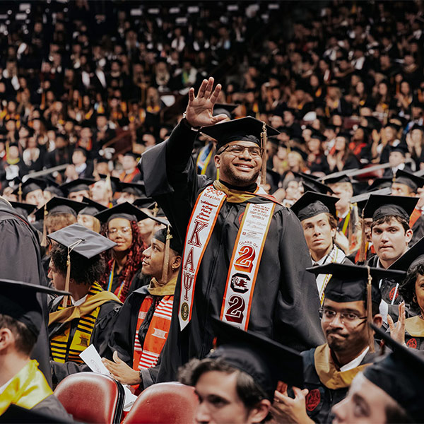
As the Class of 2026 prepares to walk across the commencement stage, graduates leave the University of South Carolina with memories of enduring friendships, newfound passions, supportive mentors and life-changing experiences.
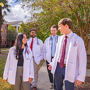
The University of South Carolina School of Medicine in Columbia is now officially named in honor of the late longtime trustee and surgeon Dr. Edward “Eddie” Floyd and his wife, Kay Floyd. The school is now known as the University of South Carolina Kay and C. Edward Floyd, M.D., School of Medicine.

Before the crowd sees him, there’s a quiet shift. The suit goes on. The posture changes. And Brayden Hensley becomes Cocky. To fans, Cocky is all energy and antics. But inside the suit is a criminology and criminal justice major balancing school and a role that demands constant performance.

You may know Cocky from game day at Williams-Brice, but some of his biggest fans sit on classroom floors, not stadium seats. Behind the yellow beak are two seniors who’ve been involved with Cocky's Reading Express for the last four years. Meet Walker Weaver and Emma Connelly.

From an early age, Stephanie Kyle had an appreciation for people from all over the world. She entertained thoughts of traveling far from South Carolina for college, but everything changed when she toured USC. As a student, she traveled widely and got involved in student organizations focused on global business and supply chain. Today, she is pricing director at a major global company.
(feat. Julia Elliott, women's and gender studies) People
(feat. David Weaver, statistics) Reasons to be Cheerful
(feat. Lorne Hofseth, drug discovery & biomedical sciences) Gizmodo
(feat Eric P. Robinson, journalism and mass communications) Media Freedom in a Changing World podcast (Indiana University)

Learn about USC's 19th Udall Scholar, Kayla Thompson, a first-generation, science-loving, rugby-playing, future environmental policy advocate. Her journey parallels that of her benefactors in many ways, and this honor motivates her to continually do more.

A decades-long fascination with life has inspired Rachel Kiser, one of two Algernon Sydney Sullivan Awards recipients, to dedicate her career to improving drug treatments for diseases.

Leadership and service is at the heart of everything Santiago Avendaño Palacio, one of two Algernon Sydney Sullivan Award recipients, does.

This spring, doctoral graduate Zo Sediqi will walk across the stage to receive her diploma from USC’s College of Education. As a woman born and raised in Afghanistan in the 1990s, the moment carries special significance: Sediqi is one of only a handful of Afghan women anywhere in the world to earn a Ph.D.