Research Step 1: Materials and Testing in Harsh Environments
Research Step 1: Materials and Testing in Harsh Environments
The first step in the development of extreme semiconductor chips is the growth and
characterization of semiconductor materials that can be used in chip fabrication.
These materials are meticulously synthesized and characterized to ensure they can
perform in a variety of extreme conditions.
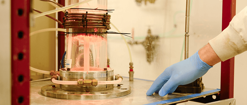
Growing and Testing Chip Materials
In this research step, we synthesize the materials to be used in the extreme semiconductor
chips, starting with growing those materials in our lab. During this process, we also
use high temperatures and harsh environments to characterize the materials.
Once the materials have been grown, an advanced materials characterization effort
will take place. Properties of the materials, such as magnetism, will be identified
using cutting-edge characterization techniques.
Project Significance
Synthesizing materials that can withstand extreme environments is the cornerstone
of developing the next generation of extreme semiconductor chips.
The characterization of these materials' properties will inform the researchers how
and if they will withstand the extreme conditions they will be used in.
Research Innovation
An innovative pulsed atomic layer epitaxy (PALE) technique will be used for the growth
of the materials for electronic and optical devices.
In-situ, high-temperature monitoring will be developed and implemented to enable the
researchers to watch the materials' reaction to extreme conditions in real time, something
that is currently lacking in other extreme semiconductor material characterization
efforts.
Research Aims
Synthesize/grow materials that can perform in extreme environments to be used in the
chips
Characterize the properties of the synthesized materials to determine how they will
react in extreme conditions
Purpose: To synthesize and characterize materials that can can withstand extreme environments
Hypothesis: The compound semiconductor AlxGa1-xN (Aluminum gallium nitride, a mixture of AlN
and GaN) is an ideal material choice
Goal: Grow and characterize materials that can be used in extreme semiconductor components
Vision:Creation and complete characterization of materials that will be used in the development
of the next generation of extreme semiconductor chips
Techniques used: Metalorganic chemical deposition (MOCVD) systems, pulsed atomic layer epitaxy (PALE), neutron-diffraction, transmission electron microscopy
The extreme semiconductors developed by our research team will lead to unprecedented
energy performance and efficiency across South Carolina. While this is a state-wide
research focus, certain areas of public interest will benefit greatly from this institute's
work.
Leadership in Innovative Technology
Our work and research puts South Carolina on the map in innumerable areas of rapidly
advancing technology. Our state will receive new opportunities and recognition by
having this world-changing technology right here at the university.
Economic Development and Engagement
A stronger reputation for technology and innovation will draw and retain more top
talent in South Carolina, creating more opportunities in multiple fields throughout
the state.
Public Health Advancements
We are changing the future of public health technology with extreme semiconductor
chips to support medical devices and products that create a better standard of care
across the state, the nation and the world—and it all starts here in South Carolina.
Comfortable Medical Wearables: With novel packaging, the extreme chips can be integrated with wearable biometric
platforms, where sensor flexibility is a key requirement for participant comfort.
Heat-Tolerant Power Electronics: By using integrated circuits that can deal with heat and electromagnetic interference,
power electronics can withstand higher temperatures.
Optical Electronics: The integration of different type of chips together will allow for extreme semiconductor
chip use in optical electronics.
Challenge the conventional. Create the exceptional. No Limits.