Research Step 2: Semiconductor Chip Design and Fabrication
Research Step 2: Semiconductor Chip Design and Fabrication
This research step starts with designing the extreme chips which are then fabricated
and tested to verify their operation in extreme environments. The result is the production
of novel, next-generation electronic and optical chips.
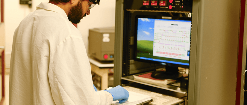
Designing and Testing the Chips
Once the synthesized materials have been grown and proven to withstand extreme environments,
this research step takes these materials and puts them into semiconductor chip designs.
Using these extreme materials, several novel electronic devices will be developed
to meet the high-power, high temperature needs of the chip application systems.
These novel devices will be tested to characterize a variety of parameters: current-voltage
(I-V) and Capacitance- voltage (C-V) parameters, high-frequency performance, high-power
switching properties, breakdown voltages and others. We will also test various light-emitting—or
optoelectronic—devices.
Project Significance
Using the synthesized extreme materials in chip designs allows for the fabrication
of semiconductor components that can perform in extreme conditions.
By characterizing multiple different chip designs and fabrications, the best designs
can be identified and used to create six key device types.
Research Innovation
In order to meet the extreme conditions where these chips need to operate, new device structures will be developed that can operate in high-power, high temperature situations.
Extreme bandgap light sources and detectors will be used to test the optoelectronic
devices.
Research Aims
Use the extreme materials in several different chip designs to fabricate possible
semiconductor components
Characterize the chip designs and fabrications to develop six key device types
Purpose: To put the synthesized materials into chip fabrications that can withstand extreme
environments
Hypothesis:Main device elements include source, gate and drain contacts and dielectric layers
that will prevent leakage currents and premature breakdown.
Goal: Semiconductor design and fabrication that perform well under extreme condition testing
Vision:Creation of six different key device types to be used in chip packaging and circuits
New device structures: Vertical conduction devices and devices with buried nanostructures, among others
The extreme semiconductors developed by our research team will lead to unprecedented
energy performance and efficiency across South Carolina. While this is a state-wide
research focus, certain areas of public interest will benefit greatly from this institute's
work.
Leadership in Innovative Technology
Our work and research puts South Carolina on the map in innumerable areas of rapidly
advancing technology. Our state will receive new opportunities and recognition by
having this world-changing technology right here at the university.
Economic Development and Engagement
A stronger reputation for technology and innovation will draw and retain more top
talent in South Carolina, creating more opportunities in multiple fields throughout
the state.
Public Health Advancements
We are changing the future of public health technology with extreme semiconductor
chips to support medical devices and products that create a better standard of care
across the state, the nation and the world—and it all starts here in South Carolina.
Comfortable Medical Wearables: With novel packaging, the extreme chips can be integrated with wearable biometric
platforms, where sensor flexibility is a key requirement for participant comfort.
Heat-Tolerant Power Electronics: By using integrated circuits that can deal with heat and electromagnetic interference,
power electronics can withstand higher temperatures.
Optical Electronics: The integration of different type of chips together will allow for extreme semiconductor
chip use in optical electronics.
Challenge the conventional. Create the exceptional. No Limits.