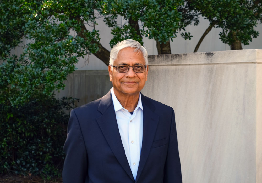
Twenty-five years ago, electrical engineering professor Asif Khan and his team helped put the University of South Carolina on the map in semiconductor electronics and photonics research, garnering several large grants and gaining widespread scholarly recognition along the way.
Khan’s research contributed heavily to the development of the multibillion-dollar LED lighting industry, and his efforts in that field were acknowledged by three Japanese scientists whose LED research earned the 2014 Nobel Prize for Physics award. Khan’s team also helped develop sensors to detect anthrax and other biological agents, as well as transistors for military radar systems and civilian cell phones. The technology developed at USC also led to the incubation of two Columbia-based small businesses (SETI Inc. and Nitek Inc.) that are among the largest commercial suppliers of ultraviolet LEDs for air and water purification.
Now, Khan and several colleagues in the Molinaroli College of Engineering and Computing are poised to do it again in the field of next-generation extreme semiconductor chips that can function in harsh environments — including outer space.
“Aluminum nitride is one of the best electrical insulator materials in the word,” says Khan, who collaborates closely with fellow electrical engineering professors Grigory Simin and Guoan Wang. “It’s a notable achievement to convert an insulator like that into a semiconductor material, and that’s what our group has done — that’s where the whole game is now. Our group and Sandia National Laboratory are the only two places in the world that have the lead in making chips from this material.”
Chips fabricated from gallium-aluminum-nitride represent the third generation of semiconductor manufacturing, an industry that began in the 1950s with silicon semiconductors and continued with second-generation gallium-arsenide chips in the 1980s. Gallium-aluminum-nitride chips can operate at high voltages and under extreme conditions, with applications including radar systems, military jets, air-water purification, biomedicine and satellites.
“We will be positioned for collaborative opportunities with top-level defense contractors who are interested in pursuing this technology.”
Khan has recently received several grants from the Department of Defense, the Department of Energy and the Defense Advanced Research Projects Agency, as well as a $4.5 million grant from the U.S. Department of Commerce to advance manufacturing techniques for such chips. To that end, renovations have begun in Khan’s Photonics Microelectronics Lab, which was built soon after his arrival in 2000 and equipped with industrial-scale equipment for materials research and chip making. The upfitting includes new manufacturing equipment that will be used to formulate semiconductor materials with varying ratios of gallium-aluminum-nitride and then turn the material into working chips.
“We have to do the research at an industrial scale so every person that we train here can go on to work in industry and not feel lost when they encounter the equipment that’s being used,” Khan says. “The other advantage of setting up our lab in this way is that we will be positioned for collaborative opportunities with top-level defense contractors who are interested in pursuing this technology.”
Khan’s team has been invited to join the Northeast Microelectronics Coalition (NEMC), which is led by the Massachusetts Technology Collaborative (MassTech) as they collaborate on a NEMC-awarded gallium nitride commercialization project led by Analog Devices, one of the largest chip manufacturers in the United States.
“My game plan is that within the next several months we'll have the best possible wafer growth laboratory infrastructure in the country at an industrial scale. We are the leader in supplying the material for the initial research,” Khan says. “And then the idea is for a large semiconductor manufacturer to take our technology and expand it to making industrial scale eight-inch wafers.”
In addition to extreme chip manufacturing technology, Khan’s research group has also made important advances in commercial ultraviolet light emitters, which are used for germ eradication, water purification and biochemical detection. Two companies were spun off from that research and both continue to operate in Columbia.
