Extreme semiconductor chips have the potential to positively impact numerous applications, such as power grids, healthcare, and military and consumer electronics, by providing unprecedented performance and efficiency.
As the materials used for semiconductor chips technology have evolved, the College of Engineering and Computing is overseeing a new institute tasked with conducting pioneering interdisciplinary research into next generation extreme semiconductor chips. The new institute aims to help enhance the quality of life in South Carolina through new businesses and economic prosperity.
Last spring, the University of South Carolina invested $10 million over four years for the Research Institutes Funding Program to provide interdisciplinary faculty research teams the funding needed for impactful progress. The Institute for Extreme Semiconductor Chips was one of five interdisciplinary research institutes established as part of the program.
The institute aims to conduct pioneering research, develop prototypes of new extreme electronic and optical chips, and establish their benefits through real-life testing. The goal is for interdisciplinary research to lead to next-generation prototype extreme chips, which can either be transferred for technological and commercial advancements to business partnerships or used as a basis to incubate new companies.
“I proposed to the university that we have expertise in materials for ultraviolet optical chips that we can also use for next generation electronic chips that can operate at extremely high powers under extreme heat and radiation conditions, says Asif Khan, institute program director and electrical engineering Carolina distinguished professor. Since semiconductor chips program is targeting to stay in the U.S., we can develop this extreme electronic chips technology at USC and serve as a local hub to work with others across the country.”
According to Khan, material systems have always been the key driver behind the evolution in semiconductor and chip technology. All electronic chips in past were based on silicon, which Khan considers first generation material. Gallium nitride and silicon carbide were second-generation electronic materials and chips based on them and their related technologies are now indispensable in any power electronics, including all major electric vehicles and computer power supplies.
I want to make this institute synonymous with the best and most innovative research in extreme semiconductors and chips in the world.
- Asif Khan
But the demands of electronics, especially intelligent power grids, require higher electronic voltages than the maximums of gallium nitride or silicon carbide. In addition to higher power and operation voltages, much higher operation speeds and much smaller footprints are also required. Subsequently, third generation technologies based on aluminum nitride material have emerged to fulfill that need.
“Most people don’t realize that in the early 2000s, USC pioneered aluminum nitride technology which was applied to optical ultraviolet LEDs. USC was the lead in incubating two companies that came out of that technology and are still operating in Columbia today,” Khan says.
This third-generation material that USC helped pioneer led Khan to consider using it to boost the power and operation voltages for operating extreme semiconductor chips. While gallium nitride can easily operate from 200 to 700 volts, power grids need anywhere from 2,000 to 5,000 volts, which are possible using extreme chips based on aluminum nitride.
“Many commercial companies are already using second generation silicon carbide and gallium nitride power electronic chips. However, the third-generation aluminum nitride electronics will not only outperform those, but it will also be radiation hard, which means these chips can easily work in space where radiation always breaks down electronics,” Khan says. “Since these materials have excellent properties in terms of high voltage and power and operate at extremely high temperatures, I decided we could use these materials to develop a new extreme chips technology.”
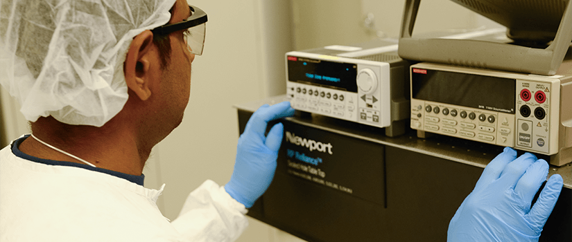
Growing and characterizing semiconductor materials that can be used in chip fabrication is the first research step in the institute’s work of developing extreme semiconductor chips. These materials are synthesized to ensure they can perform in a variety of extreme conditions. After the materials are grown and proven to withstand extreme environments, the semiconductor chip is designed and fabricated to verify operating in extreme environments. This results in the production of novel, next-generation electronic and optical chips to meet high-power and high-temperature needs. The final step is chip packaging for use in circuits of many different applications.
According to Khan, research and developing semiconductor materials for the chip technology is highly interdisciplinary. For example, chemical engineers and chemists engage in making and characterizing the materials under extreme conditions, such as ensuring semiconductor chips will work at 500 degrees Celsius. The interdisciplinary work will allow the institute to improve and modernize the technology to be brought up to the power and material of what is currently available.
“When my team of electrical engineers is growing these semiconductors, they’re essentially doing chemical engineering since the manufacturing process for materials is all chemical vapor deposition. The manufacturing and characterization processes for semiconductors are essentially materials science based. Chip making, testing and packaging is all electrical and computer engineering, and chips thermal management requires mechanical engineers,” Khan says.
The institute’s research intends to make South Carolina a nationwide hub for extreme semiconductor chip technology. The research will specifically benefit the state in leadership in innovative technology, economic development, and engagement and public health advancements.
“Since we're looking at impact and application, we want to make sure that the end users will be a part of the overall effort,” says MVS Chandrashekhar, associate professor of electrical engineering and one of the institute’s co-principal investigators. “For example, we can do studies with human participants with public health, which is something that people with semiconductors almost never do. Now, we're going to try to be more meaningful about translating our work to a real application involving public health researchers.”
With yearly goals and outcomes, Khan is confident that his team will stay on task.
“To succeed in science and technology, you must have the resources [people], and the infrastructure to solve the many pieces of the puzzle,” Khan says. “We feel that we have a good baseline infrastructure and eventually I’d like it to be upgraded to be compatible with large scale research so when it’s done, we can transfer it to a large company. It will be a seamless process because the research is already conducted on large scale equipment.”
Khan’s objectives for the institute are simple and focused. He aims to conduct the best research in extreme semiconductor chips to develop a leading-edge research group. He also wants to bring together a working group of leading researchers from other universities and industries around the country.
“I want to make this institute synonymous with the best and most innovative research in extreme semiconductors and chips in the world,” Khan says. “Along with the collaborations, I want us to be recognized as the best institute doing research into extreme semiconductor chips and material systems and evolve into a nationally recognized center.”